Unlock the Power of Nanometer-Resolution Particle Detection in Semiconductor Manufacturing
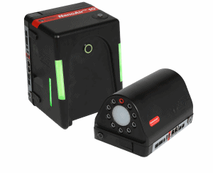
Semiconductor cleanroom processes are evolving—particle sizes that impact yield are shrinking, and traditional micron-level monitoring is no longer enough. Nanometer-resolution particle counting offers the sensitivity you need to protect critical processes and maintain production excellence. The NanoAir™ 10 condensation particle counter and ParticleSeeker™ Smart Manifold deliver reliable, actionable data at the nanometer scale, helping quality engineers enhance process control, reduce yield loss, and meet IRDS™ standards.
This technical paper dives into real-world applications through case studies, showing how nanometer-level monitoring has improved semiconductor manufacturing across multiple critical processes.
Why Nanometer Particle Detection Matters
Traditional micron-level monitoring can miss the smallest particles that impact sensitive processes. NanoAir™ 10 and ParticleSeeker™ instruments detect 10 nm particles with unmatched reliability and zero-count performance, providing insight into particle movement, tool emissions, and process impacts—all without complicating workflow.
With these tools, you can confidently:
- Optimize cleanroom and tool design for nanometer-scale contamination control
- Detect and track particle movement impacting critical wafers
- Evaluate gas and purge performance in real time
- Reduce yield loss from previously unseen nanoparticle sources
Case Studies Highlighting Airborne Nanoparticle Detection
Our study explores eight practical case studies demonstrating the use of NanoAir™ 10 and ParticleSeeker™ Instruments in semiconductor environments, including:
- Monitoring nanoparticles during spin-dry cleaning processes.
- Detecting emissions from ionizers in EFEM tools.
- Characterizing particle generation between load ports and EFEM systems.
- Monitoring nanoparticles in DUV lithography.
- Evaluating bulk gas, CDA, and parts purge performance.
Each case highlights how precise airborne nanoparticle detection enables engineers to make informed process improvements, optimize equipment design, and reduce potential yield loss.
Download the Full Paper
Discover how NanoAir™ 10 and ParticleSeeker™ Instruments are transforming airborne nanoparticle monitoring in semiconductor manufacturing.
Complete the form to download the full technical paper and explore all eight case studies in detail.