Semiconductor Particle Counting for Real-time Monitoring
Learn how semiconductor manufacturers used real-time particle monitoring to detect contamination events, investigate their sources, and support process control efforts. This paper presents two case studies and discusses key considerations for monitoring particles within semiconductor process tools.
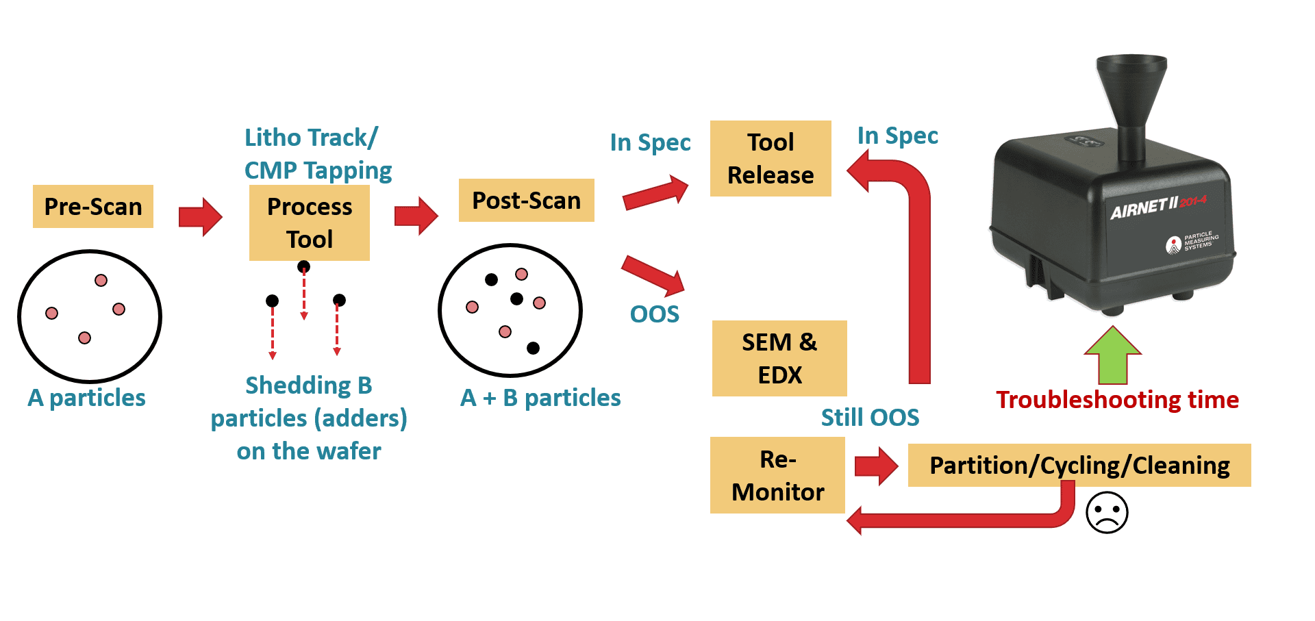
The industry of semiconductor manufacturing faces constant pressure to minimize contamination and protect wafer yield throughout complex fabrication processes. While particles are a well-known source of defects, traditional monitoring methods use inspection tools to scan the particles on control wafers. This methodology involves running the control wafers through the simulated processes. The control wafers are scanned before and after the process to calculate the particle count deposition difference between scans, aka the adder count. If the particle adder count is out of spec (OOS), the process tool must be cleaned and serviced to eliminate the particle sources until it passes the particle spec, as illustrated in the figure below.
This approach can make it difficult to quickly identify particle-generating events and determine their source within a process tool.
This paper examines how real-time aerosol particle monitoring can provide greater visibility into process tool conditions by detecting airborne particles as they are generated. It also explores the practical challenges associated with implementing particle monitoring inside semiconductor equipment, including airflow constraints, space limitations, and tool qualification requirements. Through real-world examples and technical discussion, readers will gain insight into how continuous particle monitoring can support contamination control and yield improvement efforts in semiconductor manufacturing.