20 nm Yield Protection
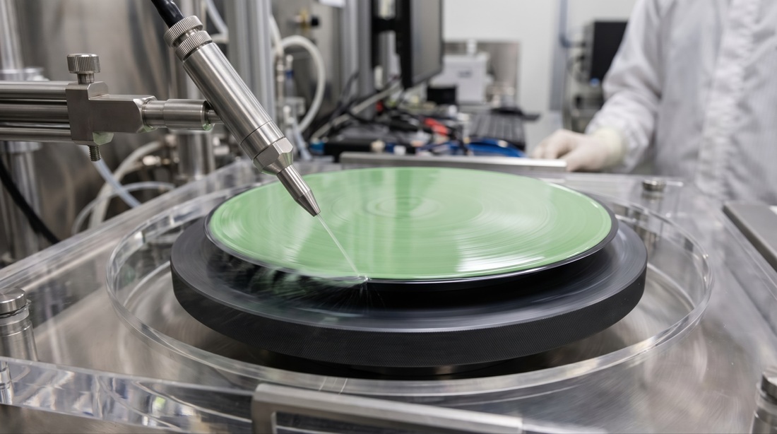
At 20 nm, contamination doesn’t just impact performance—it determines yield.
Particles at this scale are often undetectable with traditional monitoring methods, yet they can silently degrade process integrity long before defects are visible.
To operate with confidence, you need more than compliance.
You need complete visibility—and control—across your entire process.

Why 20 nm Contamination Control Matters
At advanced nodes, contamination risk is no longer isolated—it spans every stage of your process:
- Ultrapure water (UPW)
Critical to wafer cleaning, yet vulnerable to sub-visible particle contamination - Process chemicals
Highly filtered—but still capable of introducing yield-limiting particles - Distribution systems and point-of-use
Where contamination can enter undetected
At 20 nm, even trace particles can disrupt device performance and compromise yield.
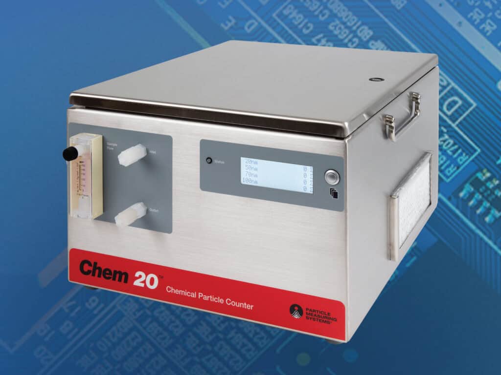
20 nm Liquid Particle Counting Solutuions
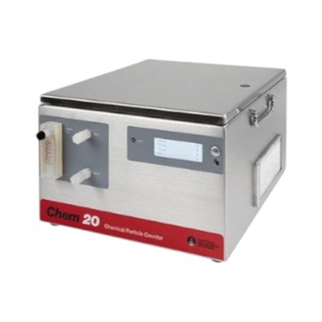
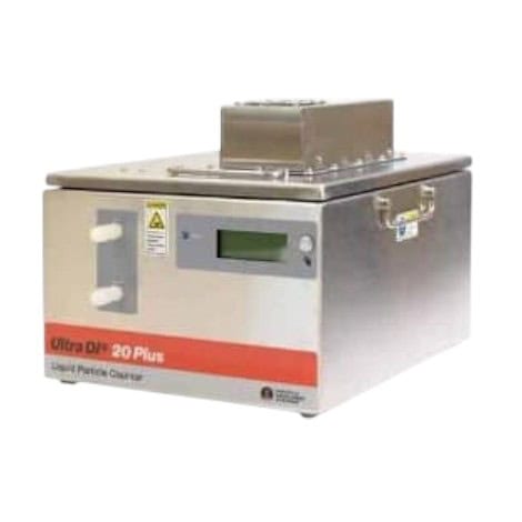
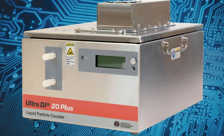
20 nm Particle Detection
Conventional particle counters lack the sensitivity required for advanced semiconductor processes.
With 20 nm particle sensitivity, PMS solutions allow you to:
- Detect contamination earlier—before yield is affected
- Identify yield-limiting particles that other systems cannot measure
- Improve process control with more accurate data
These capabilities enable proactive contamination control instead of reactive troubleshooting
Designed for Advanced Semiconductor Applications
Optimized for:
- Semiconductor fabrication facilities (fabs)
- Chemical distribution and packaging systems
- Ultrapure water (UPW) systems
- Wafer cleaning processes
Built to support:
- Process engineers
- Yield engineers
- Contamination control specialists